The Weakness of Rules of Thumb

There’s a common issue that comes up when I’m teaching people how to design electronics: people new to designing electronics often feel like they need to obey all the rules of thumb.

This came up recently when somebody I was teaching wanted to make sure none of her PCB’s electrical traces had 90 degree bends in them. There was on particular point on her board that couldn’t be made to fit that rule.

When she realized that she’d have to put a 90 degree bend in her trace, her question to me was if that was “valid and legal”. I probed her understanding a bit, and it seemed she was mostly thinking about the design guidelines as though they were laws, and she didn’t want her design to break any laws.

This kind of thinking is pretty common, but I think it actively prevents people from designing electronics effectively. People with this mindset focus too much on whether their design meets some set of rules, and not enough on whether their design will actually work.

Where Design Guidelines Come From

Electronics is a domain that has a lot of rules of thumb. There are some pretty complicated physics behind how electrons act on a circuit board, and you can often simplify an engineering problem to a simple rule.

After a few decades of the industry doing this, there’s a large collection of rules. New engineers sometimes learn the rules before learning the physical principles that drive them, and then don’t know when the rules don’t apply.

For example, the advice to not put 90 degree bends in electrical traces is due to the fact that sharp bends increase the reactive impedance of a trace. For high frequency traces, this can distort the electrical signal flowing down the trace.

For low frequency or DC signals, 90 degree bends are much less of an issue.

Ultimately, any rule of thumb rests on a concrete foundation of “if this condition holds, then that result will be produced in a specific manner”. If you know the detailed model that drives the simple rule, you know when to ignore the rule.

Obeying The Rules or Designing a Working Project

The mindset that I sometimes see in new students is the idea that they need to follow all the rules. This makes sense if you assume that following all the rules will automatically lead to a working project. Unfortunately, the rules of thumb in electronics over-constrain a circuit board. Electrical engineers will often face the prospect of a design guideline that can’t be satisfied.

The most effective response to a rule of thumb that can’t be satisfied seems to be to ask about the physics behind the rule. Then the engineer can figure out how change the design to match the physical laws behind the general guideline.

The design guidelines were made for the people, not the people for the design guidelines.

Don’t ask “how can I make this design satisfy all the design guidelines?”

Instead ask “how can I make this design work?”

Non-binary memory based on quantum effects

NAND Flash memory is made using floating gate transistors. This means that the gates to the transistors are electrically isolated from any other contact on the transistor. Quantum tunneling is used to deposit electrons on the gate, changing the transistor state. When many electrons are located on the gate, the transistor is on and stores a logical 1. When the gate has few electrons, the transistor is off and stores a logical 0. Changing the number of electrons on the gate is done by applying a voltage across the gate that sufficient to induce electron tunneling between an electrode and the isolated gate.

Newer forms of NAND flash actually store multiple bits on each transistor. Different levels of electrons on the gate correspond to different values, and the number of bits represented corresponds to the different number of discern-able electron levels (n bits = log2(n) electron levels).

A lot of thumb drives are made using NAND flash, which means people are just carrying around non-binary memory that makes use of quantum effects.

I think it’s pretty clear that we already live in the future.

parts.io

parts.io is a new parametric search engine for parts. Supposedly it’s claim to fame is that it finds parts from all distributors (like octopart) and presents a more complete picture on the lifecycle status of a part (super important). It seems to have promise, but I don’t think it’s better than digikey yet.

I liked the way parts.io presented information. After I make a selection in digikey, it can be hard to undo it or find out what selection I even made. The UI for parts.io is definitely better.

My main problem with parts.io is that it doesn’t seem to know very much about electronics. If I’m making an RF filter, I can’t use general purpose capacitors for it. Digikey makes it easy to select only RF rated capacitors. Parts.io doesn’t even seem to know the difference exists.

Parts.io also has a units problem. Large or small part values are displayed in scientific notation with no units. The standard prefixes (k for kilo, M for mega, etc.) sometimes aren’t recognized by their search engine. It also turns out capacitances are displayed in uF only, which is somewhat non-standard.

parts.io seems to have the right idea, but I’ll wait until they’re out of alpha to actually start using them.

LG HBS 700 Wireless Headphones Teardown

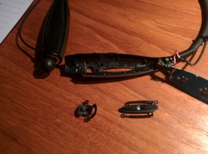
A friend gave me his broken pair of LG HBS 700 wireless headphones a while ago, and I finally got around to tearing them down.

headphones before teardown

Housing

The housing for these headphones is made up of two cavities on either side of the head. One side holds the battery, and the other holds pretty much everything else. The semi-rigid band connecting the two cavities contains wires for audio, power, and the several buttons on the non-circuitry side.

The buttons are plastic parts with supports on two sides. The supports deform, allowing pegs on the bottom of the buttons to depress electrical switches mounted on the PCB.

buttons from left cavity of housing

The housing also has cups to hold the headphones when they’re not being used. The cups have magnets in them, which is pretty cool. Headphones already have magnets in them for the speakers, so this is a nice use of an incidental property of the speaker.

Left Cavity

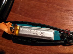
The Left cavity contains the battery, three switches, and the left headphone. The audo for the left headphone comes directly from the right cavity, but the audio wires from the right cavity are soldered onto the left PCB. The left headphone is also soldered onto the left PCB, and the audio is routed through a couple of ~1cm traces. I’m assuming that they did that for ease of assembly. That way they only need one type of headphone pigtail.

battery in left cavity

The battery doesn’t have many markings, but based on its size I’d guess it’s about 200mAh to 220mAh.

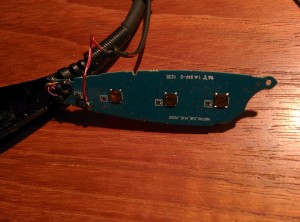
The PCB in the left cavity has three buttons on it. These buttons look to be PTS530 buttons or something similar.

buttons on left PCB

Right Cavity

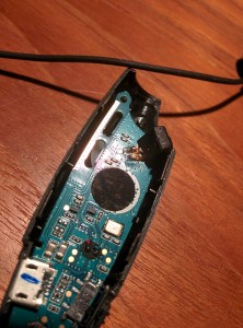
The PCB in the right cavity has all the main circuitry in these headphones. The USB jack is mounted on the bottom, along with vibrating motor, on/off switch, 26MHz oscillator for the BT IC, microphone, and a bunch of passives.

Bottom of main PCB

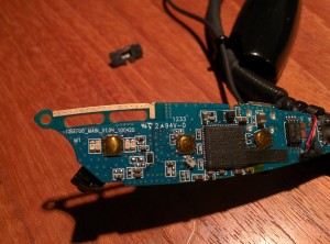
The top of the main PCB has three buttons, one of them canted slightly to make it fit. There’s also a 8pin SOIC that’s probably an EEPROM. The other main component on this board is the SoC handling pretty much all of the features of the device.

top of main PCB

The SoC is a CSR57F68. I couldn’t find this part on the CSR web site, but based on this circuit I think it’s safe to say it has integrated BT radio, battery charging, audio DAC and ADC with amplifiers, as well as a microcontroller core.

RF

I have a bit of experience with BT antennas, but RF is definitely not my expertise. I was pretty interested to see the RF hardware in this device, and there were a few surprises.

The antenna in these headphones is looks to be an inverted-L antenna. Interestingly, the antenna trace is routed on both sides of the board with vias connecting the sides. The edge of the PCB is also copper-clad. I’m assuming this was done to increase the radiation resistance of the antenna. Although it may have been done to push the impedance of the antenna closer to 50 Ohms.

The trace feeding the antenna is pretty long, and has a couple of 45deg angles in it. There’s good stitching of the ground plane on one side of that trace, but not on the other (presumably because there are traces there on another layer). There are also a few fat traces (probably power) going directly underneath the antenna trace. From the looks of the board, there’s a ground plane between the antenna trace and the power traces, so that’s probably not causing any interference.

The feedline for the antenna is driven by the CSR chip through what looks to be a pretty standard balun.

One interesting things about this device is that there’s no metal can over the RF components. Instead, they used a piece of conductive tape. The tape, which is a square the size of the CSR chip with a little tail, is placed over CSR chip. The tail trails off to a portion of the ground plane with the soldermask removed, thus providing a ground plane above the CSR chip as well.

This conductive tape tail passes over a couple of components and traces to get to the ground plane. To protect those components from being shorted to ground, there’s a small piece of kapton tape between the conductive tape and the components.

This seems like a pretty finicky thing to do in manufacturing, and I can’t help but think that they could have saved some money by re-designing the board to move those components.

My hypothesis is that they realized they had an EMI problem late in design after they’d already tooled up. I bet they just made a small change to the soldermask layer and left the programming for the Pick and Place machines the same. The conductive tape was probably just an emergency measure.

I’d be interested in checking out a later version of these headphones to see if they have the same tape solution.

Microphone

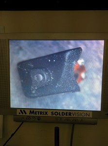
The microphone on these headphones is encapsulated in a rubber case. I’m guessing they cast the rubber case as a tube, put the microphone in the back of the tube, and then epoxied over it. That provides a waveguide for the audio from outside the housing directly to the microphone.

Microphone in housing, viewed head-on to the audio port.

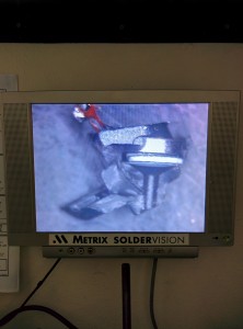
The microphone itself looks like a standard electret microphone. The rubber case forms a kind of funnel. I cut the rubber case in half to see how it was formed internally.

Audio channel through the rubber microphone case.

The audio channel in the rubber microphone case is fairly narrow where it meets the external world. I’m assuming that was done to prevent water from getting in and ruining things. The aperture then widens to the total size of the microphone. Sometimes these chambers can act as Helmholtz resonators, but I think that in this case that won’t happen. Because the microphone itself makes up the entirety of the back wall of the chamber, all of the sound energy is probably absorbed by the microphone instead of resonating.

KiCAD libraries

I’ve been using KiCAD for my schematic capture and layout tasks for about a year now, and I find it to be the best free tool that I’ve seen. In the interest of making it easier to share my projects, I’ve put all of my KiCAD libraries on github: https://github.com/mogar/KiCAD_libs

I tend to organize my libraries in pairs. One library of symbols and one library of corresponding modules. That way I know where to find the footprint I’m looking for.

I started out using a library that had been created from the SparkFun Eagle libraries. This has worked pretty well and has a lot of common components, but footprints are often messed up. I’ve been fixing them as I run into issues, but definitely check all footprints from the library before you use it.

The other libraries have parts that I haven’t found in the SparkFun library. Those libraries are better maintained, but I still suggest you double check everything before using any of those parts.