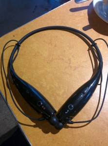
A friend gave me his broken pair of LG HBS 700 wireless headphones a while ago, and I finally got around to tearing them down.
Housing
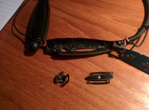
The housing for these headphones is made up of two cavities on either side of the head. One side holds the battery, and the other holds pretty much everything else. The semi-rigid band connecting the two cavities contains wires for audio, power, and the several buttons on the non-circuitry side.
The buttons are plastic parts with supports on two sides. The supports deform, allowing pegs on the bottom of the buttons to depress electrical switches mounted on the PCB.
The housing also has cups to hold the headphones when they’re not being used. The cups have magnets in them, which is pretty cool. Headphones already have magnets in them for the speakers, so this is a nice use of an incidental property of the speaker.
Left Cavity
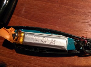
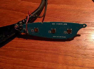
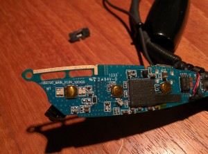
The Left cavity contains the battery, three switches, and the left headphone. The audo for the left headphone comes directly from the right cavity, but the audio wires from the right cavity are soldered onto the left PCB. The left headphone is also soldered onto the left PCB, and the audio is routed through a couple of ~1cm traces. I’m assuming that they did that for ease of assembly. That way they only need one type of headphone pigtail.
The battery doesn’t have many markings, but based on its size I’d guess it’s about 200mAh to 220mAh.
The PCB in the left cavity has three buttons on it. These buttons look to be PTS530 buttons or something similar.
Right Cavity
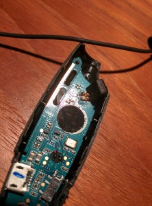
The PCB in the right cavity has all the main circuitry in these headphones. The USB jack is mounted on the bottom, along with vibrating motor, on/off switch, 26MHz oscillator for the BT IC, microphone, and a bunch of passives.
The top of the main PCB has three buttons, one of them canted slightly to make it fit. There’s also a 8pin SOIC that’s probably an EEPROM. The other main component on this board is the SoC handling pretty much all of the features of the device.
The SoC is a CSR57F68. I couldn’t find this part on the CSR web site, but based on this circuit I think it’s safe to say it has integrated BT radio, battery charging, audio DAC and ADC with amplifiers, as well as a microcontroller core.
RF
I have a bit of experience with BT antennas, but RF is definitely not my expertise. I was pretty interested to see the RF hardware in this device, and there were a few surprises.
The antenna in these headphones is looks to be an inverted-L antenna. Interestingly, the antenna trace is routed on both sides of the board with vias connecting the sides. The edge of the PCB is also copper-clad. I’m assuming this was done to increase the radiation resistance of the antenna. Although it may have been done to push the impedance of the antenna closer to 50 Ohms.
The trace feeding the antenna is pretty long, and has a couple of 45deg angles in it. There’s good stitching of the ground plane on one side of that trace, but not on the other (presumably because there are traces there on another layer). There are also a few fat traces (probably power) going directly underneath the antenna trace. From the looks of the board, there’s a ground plane between the antenna trace and the power traces, so that’s probably not causing any interference.
The feedline for the antenna is driven by the CSR chip through what looks to be a pretty standard balun.
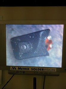
One interesting things about this device is that there’s no metal can over the RF components. Instead, they used a piece of conductive tape. The tape, which is a square the size of the CSR chip with a little tail, is placed over CSR chip. The tail trails off to a portion of the ground plane with the soldermask removed, thus providing a ground plane above the CSR chip as well.
This conductive tape tail passes over a couple of components and traces to get to the ground plane. To protect those components from being shorted to ground, there’s a small piece of kapton tape between the conductive tape and the components.
This seems like a pretty finicky thing to do in manufacturing, and I can’t help but think that they could have saved some money by re-designing the board to move those components.
My hypothesis is that they realized they had an EMI problem late in design after they’d already tooled up. I bet they just made a small change to the soldermask layer and left the programming for the Pick and Place machines the same. The conductive tape was probably just an emergency measure.
I’d be interested in checking out a later version of these headphones to see if they have the same tape solution.
Microphone
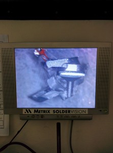
The microphone on these headphones is encapsulated in a rubber case. I’m guessing they cast the rubber case as a tube, put the microphone in the back of the tube, and then epoxied over it. That provides a waveguide for the audio from outside the housing directly to the microphone.
The microphone itself looks like a standard electret microphone. The rubber case forms a kind of funnel. I cut the rubber case in half to see how it was formed internally.
The audio channel in the rubber microphone case is fairly narrow where it meets the external world. I’m assuming that was done to prevent water from getting in and ruining things. The aperture then widens to the total size of the microphone. Sometimes these chambers can act as Helmholtz resonators, but I think that in this case that won’t happen. Because the microphone itself makes up the entirety of the back wall of the chamber, all of the sound energy is probably absorbed by the microphone instead of resonating.
